[{1 1}]
2024-07-09
6576
The evolution of digital electronics has been shaped by the development of Complementary Metal-Oxide-Semiconductor (CMOS) technology. Emergent in response to the need for faster processing speeds and more efficient power consumption, CMOS technology has revolutionized circuit design with its innovative approach to managing power and signal integrity. Unlike the Bipolar Junction Transistor (BJT) devices, which are dependent on current flow, CMOS devices utilize voltage-controlled mechanisms that significantly reduce gate current, thereby minimizing power loss. This technology first gained traction in consumer electronics in the 1970s, such as in electronic watches, but it was the advent of Very-Large-Scale Integration (VLSI) in the 1980s that truly cemented the position of CMOS as a cornerstone in modern electronics. The era witnessed CMOS technology enhancing circuit reliability, noise resistance, and performance across varying temperatures and voltages while simplifying the overall design process. These enhancements not only increased the transistor count from thousands to millions on a single chip but also extended the functionality of CMOS to both digital and mixed-signal VLSI designs, outperforming older technologies like Transistor-Transistor Logic (TTL) due to its superior speed and lower voltage operations.
Catalog
Understanding of CMOS Technology
The development of Complementary Metal-Oxide-Semiconductor (CMOS) technology has been huge part in advancing digital circuit design. It emerged mainly due to the need for faster processing and lower energy consumption. Unlike Bipolar Junction Transistor (BJT) devices, which depend on current flow, CMOS uses voltage-controlled mechanisms. The major difference helps reduce the current at the gate, cutting down power loss significantly. In the 1970s, CMOS was mainly used in consumer electronics, such as electronic watches.
The landscape changed in the 1980s with the advent of Very-Large-Scale Integration (VLSI) technology, which heavily adopted CMOS for several reasons. CMOS uses less power, offers better noise resistance, and performs well across various temperatures and voltages. It also simplifies circuit design which increases reliability and flexibility. These features allowed a huge increase in the integration density of CMOS-based chips, moving from thousands to millions of transistors per chip.
Today, CMOS is useful to both digital and mixed-signal VLSI designs, outperforming older technologies like Transistor-Transistor Logic (TTL) due to its superior speed and efficiency at lower voltages. Its widespread use highlights CMOS's transformative impact on modern electronics, making it the go-to technology for everything from everyday gadgets to advanced computational systems.

Figure 1: Use to Balance Electrical Characteristics
Working Principle of CMOS
The core principle of Complementary Metal-Oxide-Semiconductor (CMOS) technology uses a pair of N-type and P-type transistors to create efficient logic circuits. A single input signal controls the switching behavior of these transistors, turning one on while turning the other off. This design eliminates the need for traditional pull-up resistors used in other semiconductor technologies, simplifying the design and improving energy efficiency.
In a CMOS setup, N-type MOSFETs (Metal-Oxide-Semiconductor Field-Effect Transistors) form a pull-down network connecting the output of the logic gate to a low voltage supply, usually ground (Vss). This replaces the load resistors in older NMOS logic circuits, which were less effective at managing voltage transitions and more prone to power loss. Conversely, P-type MOSFETs create a pull-up network that connects the output to a higher voltage supply (Vdd). This dual-network arrangement ensures that the output is controlled stably and predictably for any given input.
When the gate of a P-type MOSFET is activated, it switches on while the corresponding N-type MOSFET switches off, and vice versa. This interplay not only simplifies the circuit architecture but also enhances the operational reliability and functionality of the device. CMOS technology is beneficial for users who need dependable and efficient electronic systems.
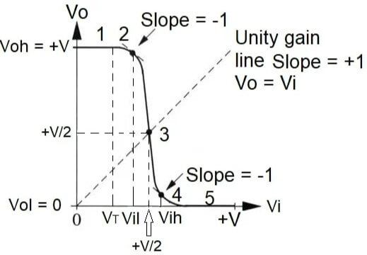
Figure 2: Introduction to CMOS Tech
The Inverter
The inverter is a primary element in digital circuit design, particularly for binary arithmetic and logical operations. The main function is to reverse the input signal within binary logic levels. In simple terms, a '0' is considered low or zero volts, and a '1' is high or V volts. When an inverter receives an input of 0 volts, it outputs V volts, and when it receives V volts, it outputs 0 volts.
A truth table typically demonstrates the inverter's function by listing all possible inputs and their corresponding outputs. This table clearly shows that an input of '0' produces an output of '1', and an input of '1' results in an output of '0'. This inversion process is required for logical decisions and data processing in computing and digital systems.
The inverter's operation is required for more complex digital interactions. It enables the smooth execution of higher-level computational tasks and helps manage data flow within circuits effectively.
|
INPUT |
OUTPUT |
|
0 |
1 |
|
1 |
0 |
Table 1: Inverter Truth Table
The CMOS Inverter
The CMOS inverter is a model of efficiency in electronics, featuring a simple design with NMOS and PMOS transistors connected in series. Their gates are tied together as the input, and their drains are connected to form the output. This arrangement reduces power dissipation, optimizing the circuit for energy efficiency.
When the input signal is high (logic '1'), the NMOS transistor turns on, conducting current and pulling the output to a low state (logic '0'). At the same time, the PMOS transistor is off, isolating the positive supply from the output. Conversely, when the input is low (logic '0'), the NMOS transistor turns off, and the PMOS transistor turns on, driving the output to a high state (logic '1').
This coordination between the NMOS and PMOS transistors allows the inverter to maintain stable output despite input voltage variations. By ensuring that one transistor is always off while the other is on, the CMOS inverter conserves power and prevents a direct electrical path from the power supply to the ground. It will help prevent unnecessary power drain. This dual-transistor setup defines the CMOS inverter’s primary role in digital circuitry, providing reliable logic inversion with minimal energy consumption and high signal integrity.
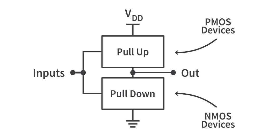
Figure 3: CMOS Logic Gates
The NMOS Inverter
The NMOS inverter is built using a straightforward and efficient setup. In this configuration, the gate serves as the input, the drain functions as the output, and both the source and substrate are grounded. The core of this arrangement is an enhancement-type n-channel MOSFET. A positive voltage is applied to the drain through a load resistor to establish the right biasing.
When the gate input is grounded, representing a logic '0', no voltage is present at the gate. This lack of voltage prevents a conductive channel from forming in the MOSFET, making it an open circuit with high resistance. As a result, minimal current flows from the drain to the source, causing the output voltage to rise close to +V, which corresponds to a logic '1'. When a positive voltage is applied to the gate, it attracts electrons to the gate oxide interface, forming an n-type channel. This channel reduces the resistance between the source and drain, allowing the current to flow and drop the output voltage to nearly ground level, or logic '0'.
This operation shows the NMOS inverter as an effective pull-down device, useful for binary switching tasks. It is helpful to recognize that this setup tends to consume more power when in the 'on' state. The increased power consumption arises from the continuous current flowing from the power supply to the ground when the transistor is active, highlighting a key operational trade-off in the NMOS inverter design.
The PMOS Inverter

Figure 4: CMOS ICs Basics
The PMOS inverter is structured similarly to the NMOS inverter but with reversed electrical connections. In this setup, a PMOS transistor is used with a positive voltage applied to both the substrate and source, while the load resistor is connected to the ground.
When the input voltage is high at +V (logic '1'), the gate-to-source voltage becomes zero, turning the transistor 'off'. This creates a high resistance path between the source and drain, keeping the output voltage low at logic '0'.
When the input is at 0 volts (logic '0'), the gate-to-source voltage becomes negative relative to the source. This negative voltage charges the gate capacitor, inverting the semiconductor surface from n-type to p-type, and forming a conductive channel. This channel drastically lowers the resistance between the source and drain, allowing current to flow freely from the source to the drain. As a result, the output voltage rises close to the supply voltage +V, corresponding to a logic '1'.
In this way, the PMOS transistor acts as a pull-up device, which provide a low resistance path to the positive supply voltage when activated. This makes the PMOS inverter a primary component in creating stable and reliable logic inversion. It ensures that the output is strongly driven to the high state when required.
Cross Section of a CMOS

Figure 5: Cross Section of CMOS Gate
A CMOS chip combines NMOS and PMOS transistors on a single silicon substrate, forming a compact and efficient inverter circuit. Viewing a cross-section of this setup shows the strategic placement of these transistors, optimizing functionality and reducing electrical interference.
The PMOS transistor is embedded in the n-type substrate, while the NMOS transistor is placed in a separate p-type area called the p-well. This arrangement ensures that each transistor operates under optimal conditions. The p-well acts as the operational ground for the NMOS transistor and isolates the electrical paths of the NMOS and PMOS transistors, preventing interference. This isolation is helpful to maintain signal integrity and overall CMOS circuit performance.
This configuration allows the chip to switch between high and low logic states quickly and reliably. By integrating both types of transistors in one unit, the CMOS design balances their electrical characteristics, leading to more stable and efficient circuit operations. This integration reduces the size and improves the performance of modern electronic devices, showcasing the advanced engineering behind CMOS technology.
Power Dissipation of a CMOS Inverter
A key feature of CMOS technology is its efficiency in power dissipation, especially in static or idle states. When inactive, a CMOS inverter draws very little power since the "off" transistor leaks only a minimal current. This effectiveness is helpful to maintain the energy waste and extending the battery life of portable devices.
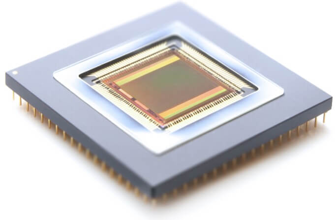
Figure 6: CMOS Sensors- for Industrial Cameras
During dynamic operation, when the inverter switches states, power dissipation temporarily increases. This spike occurs because, for a brief moment, both the NMOS and PMOS transistors are partially on, creating a short-lived direct path for current flow from the supply voltage to the ground. Despite this transient increase, the overall average power consumption of a CMOS inverter remains much lower than that of older technologies like Transistor-Transistor Logic (TTL).
This sustained low power usage across different operational modes enhances the energy efficiency of CMOS circuits. Making it ideal for applications where power availability is limited, such as mobile devices and other battery-powered technologies.
The low steady-state power draw of CMOS inverters generates less heat which reduces thermal stress on device components. This reduced heat generation can prolong the lifespan of electronic devices, making CMOS technology a key factor in designing more sustainable and cost-effective electronic systems.
The DC Voltage Transfer Characteristic of the CMOS Inverter
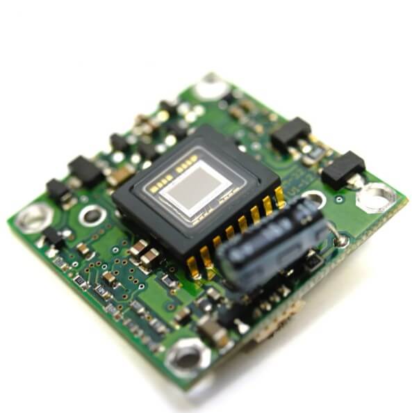
Figure 7: Optimize Circuits for Power and Speed Efficiency
The DC voltage transfer characteristic (VTC) of a CMOS inverter is a primary tool to understand its behavior. It shows the relationship between input and output voltages in static (non-switching) conditions, providing a clear view of the inverter's performance across different input levels.
In a well-designed CMOS inverter, where the NMOS and PMOS transistors are balanced, the VTC is nearly ideal. It is symmetrical and has a sharp transition between high and low output voltages at a specific input voltage threshold. This threshold is the point where the inverter switches from one logic state to another, quickly changing from logic '1' to '0' and vice versa.
The precision of the VTC is helpful to determine the operational voltage ranges of digital circuits. It identifies the exact points where the output will change states, ensuring that logic signals are clear and consistent, and reducing the risk of errors due to voltage variations.
Advantages of CMOS Technology
CMOS technology offers low static power consumption. Making it more useful for electronic applications, especially in battery-powered devices, as it uses energy only during logic state transactions.
The design of CMOS circuits inherently simplifies complexity, allowing a compact, high-density arrangement of logic functions on a single chip. This feature is required to enhance microprocessors and memory chips, improving operational capabilities without expanding the physical size of the silicon. This density advantage allows for more processing power per unit area, facilitating advancements in technology miniaturization and system integration.
CMOS technology’s high noise immunity reduces interference, ensuring stable and reliable operation of CMOS-based systems in electronic noise-prone environments. The combination of low power consumption, reduced complexity, and robust noise immunity solidifies CMOS as a foundational technology in electronics. It supports a wide range of applications, from simple circuits to complex digital computing architectures.

Figure 8: CMOS Technology Diagram
A Recap of CMOS Technology
CMOS technology is a cornerstone of modern digital circuit design, using both NMOS and PMOS transistors on a single chip. This dual-transistor approach enhances efficiency through complementary switching and reduces power consumption, which is beneficial in today's energy-conscious world.
The strength of CMOS circuits comes from their low power requirements and excellent noise immunity. These traits are useful to create a reliable and complex digital integrated circuit. CMOS technology effectively resists electrical interference, improving the stability and performance of electronic systems.
CMOS's low static power consumption and reliable operation make it the preferred choice for many applications. From consumer electronics to high-end computing systems, CMOS technology's adaptability and efficiency continue to drive innovation in the electronics industry. Its widespread use highlights its importance in advancing digital technology.
Conclusion
CMOS technology stands as a paragon of innovation in the field of digital circuit design, continually driving the advancement of electronics from basic gadgets to complex computational systems. The dual-transistor setup of NMOS and PMOS on a single chip allowed for efficient switching, minimal power dissipation, and a high degree of noise immunity, making CMOS useful in the creation of dense, integrated circuits. Reducing power consumption without sacrificing performance has proven in the era of portable, battery-powered devices. The robustness of CMOS technology in handling various operational and environmental conditions has broadened its applications across numerous domains. As it continues to evolve, CMOS technology can help shape the future landscape of electronic design. It ensures t remain at the forefront of technological innovation and continues to meet the increasing demands for energy efficiency and miniaturization in electronic devices.
Frequently Asked Questions [FAQ]
Q1. How does CMOS work in digital electronics?
Complementary Metal-Oxide-Semiconductor (CMOS) technology is foundational in digital electronics, primarily because it efficiently controls the flow of electricity in devices. In practice, a CMOS circuit includes two types of transistors: NMOS and PMOS. These are arranged to ensure that only one of the transistors conducts at a time, which drastically reduces the energy consumed by the circuit.
When a CMOS circuit is in operation, one transistor blocks current while the other lets it pass. For example, if a digital signal of '1' (high voltage) is input into a CMOS inverter, the NMOS transistor turns on (conducts), and the PMOS turns off (blocks current), resulting in a low voltage or '0' at the output. Conversely, an input of '0' activates the PMOS and deactivates the NMOS, resulting in a high output. This switching ensures minimal power is wasted, making CMOS ideal for devices like smartphones and computers where battery efficiency is required.
2. What is the difference between MOSFET and CMOS?
MOSFET (Metal-Oxide-Semiconductor Field-Effect Transistor) is a type of transistor used for switching electronic signals. CMOS, on the other hand, refers to a technology that utilizes two complementary types of MOSFETs (NMOS and PMOS) to create digital logic circuits.
The primary distinction lies in their application and efficiency. A single MOSFET can function as a switch or amplify signals, requiring a continuous flow of power and potentially generating more heat. CMOS, by integrating both NMOS and PMOS transistors, alternates between using one or the other, reducing the power required and heat generated. This makes CMOS more suitable for modern electronic devices that require high efficiency and compactness.
3. What happens if you clear CMOS?
Clearing the CMOS on a computer resets the BIOS (Basic Input/Output System) settings to their factory defaults. This is often done to troubleshoot hardware or boot problems that may arise due to incorrect or corrupted BIOS settings.
To clear CMOS, you typically short a specific pair of pins on the motherboard using a jumper, or remove the CMOS battery for a few minutes. This action flushes the volatile memory in the BIOS, erasing any configurations such as boot order, system time, and hardware settings. After clearing the CMOS, you may need to reconfigure the BIOS settings according to your computing needs or hardware compatibility.
4. What will replace CMOS?
While CMOS technology is still prevalent, ongoing research aims to develop alternatives that could potentially offer greater efficiency, speed, and integration as technology scales down further.
Graphene Transistors are being explored for their exceptional electrical properties, such as higher electron mobility than silicon, which could lead to faster processing speeds.
Utilizes quantum bits that can exist in multiple states simultaneously, offering exponential speed increases for specific computations.
Spintronics: Uses the spin of electrons, rather than their charge, to encode data, potentially reducing power consumption and increasing data processing capabilities.
While these technologies are promising, transitioning from CMOS to a new standard in digital electronics will require overcoming technical challenges and substantial investments in new manufacturing technologies. As of now, CMOS remains the most practical and widely used technology in digital circuit design due to its reliability and cost-effectiveness.
 FAATATAU IA TATOU
Tagata faamalieina i taimi uma.Agaalofa ma le talitonuina ma fiafia masani.
suʻega suʻega.O oloa aupito pito sili ona maualuga tau ma le tautua sili o lo tatou tautinoga faavavau.
![[{1 1}]](/upfile/blog/small_2024070916310837321.png) [{1 1}]
[{1 1}]
2024-07-09
![[{1 1}]](/upfile/blog/small_2024070914285948631.png) [{1 1}]
[{1 1}]
2024-07-09
VAI VAEGA Numera
 C3225X8R1E225K200AA
 GRM0225C1ER60BDAEL
 GRM1555C1H300GA01D
 CL05A224MP5NNNC
 CL10C2R2BB8NNNL
 AMK042BJ473KC-W
 GRM3195C1E103JA01J
 CS0603KRX7R9BB391
 08053C331JAZ2A
 12067A561GAT2A
- T491B107M010AT
- 1060-16-0144
- NFM3DCC222R1H3L
- CY22050FZXC
- X1205S8ZT1
- MCC5E0RX266WB0B
- VI-203-IX
- MAX530BCAG
- LFE2M35SE-5FN484C
- HV9910BNG-G
- VOS628A-2X001T
- S1A
- VI-260-CW
- 1MBI600PX-140-03
- LM3480IM3-15/NOPB
- TMX320DM8148BCYE
- XC7A35T-1CPG236I
- UCC38C43DGKRG4
- LT1940EFE#PBF
- ADS7861E/2K5G4
- T491A475K016AT4860
- T491C106M025AH
- A20
- CM600DU-24NF#300G
- DP7113ZI-10-TE3
- FSTU6800
- GAL22LV10-7LJ
- HPFC-6750C
- PBL38620/2R2
- TC74VHC21FS
- TPS2202AIDBLE
- UJA1061TW/5V0/C/T
- XR16L788CQ
- RTL8102E-VB-GR
- APW7145KAI-TRL
- TRF6150PAP
- TMP93CS32FG6KG5
- DAC7664Y
- SDFL2012S100KTF